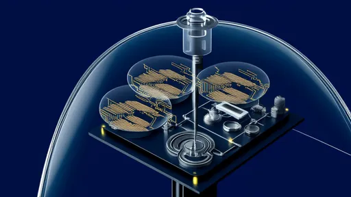
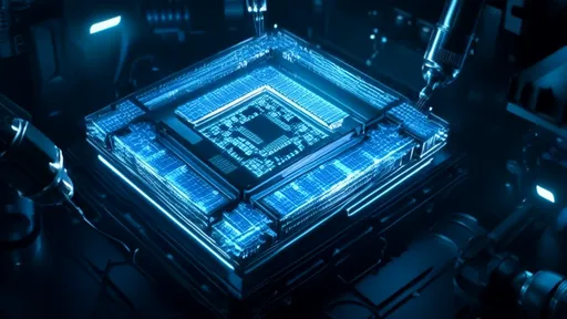
For decades, the computing industry has been shackled by the von Neumann bottleneck, the fundamental latency and energy inefficiency caused by shuttling data between separate memory and processing units. This architectural constraint has become increasingly problematic in the age of big data and artificial intelligence, where processing vast datasets in real-time is paramount. A paradigm shift is underway, moving computation from the processor directly into the memory array itself. This is the promise of In-Memory Computing (IMC), a technology long confined to research labs and theoretical papers that is now decisively stepping out of the prototype phase and into the commercial arena.
The journey from academic concept to tangible product has been a long and arduous one. Early prototypes, often built on exotic materials and complex fabrication processes, demonstrated compelling proof-of-concept but were far from being manufacturable at scale. Researchers grappled with issues of variability, endurance, and the sheer difficulty of integrating novel memory elements with standard CMOS logic. For years, IMC was a solution in search of a problem that couldn't be solved by simply throwing more transistors and more advanced process nodes at it. That problem has now arrived with undeniable force. The insatiable computational demands of deep learning, particularly for inference at the edge, and the physical limits of traditional scaling have created a perfect storm, making the industry desperately seek alternatives.
Key players, from agile startups to semiconductor titans, are now placing their bets. Startups like Mythic and Syntiant focused early on analog in-memory computing using non-volatile memory technologies to create ultra-low-power accelerators for always-on AI in edge devices. Their progress from securing venture capital to delivering first-generation chips to customers marks a critical inflection point. It signals that the market sees viable paths to production and application. Meanwhile, established giants are not sitting idle. Samsung and SK Hynix, lords of the memory domain, are actively exploring Processing-In-Memory (PIM) architectures, embedding simple compute capabilities within DRAM or High-Bandwidth Memory (HBM) to alleviate data movement bottlenecks for data-intensive workloads in servers and GPUs. Even Intel and IBM have showcased advanced research prototypes, indicating a broad industry belief that this is a cornerstone for future computing.
The technology is maturing along multiple parallel paths. The debate between analog and digital implementations of IMC is a central one. Analog IMC, which uses the physical properties of memory devices like resistive RAM (ReRAM) or phase-change memory (PCM) to perform multiplication-and-accumulation (MAC) operations—the core of neural network math—promises revolutionary energy efficiency. However, it must overcome challenges related to computational precision, noise, and device drift. Digital IMC, which places simpler processing elements bit-serial adders or look-up tables inside or adjacent to the memory array, offers deterministic, bit-accurate results but may sacrifice some degree of energy efficiency. The choice of memory technology itself—ReRAM, PCM, MRAM, or even modified SRAM and DRAM—creates a rich and complex landscape of trade-offs between speed, density, endurance, and ease of integration with existing foundry processes.
This commercial translation is being fueled by a specific and urgent market pull: artificial intelligence. The training of massive models like GPT-4 grabs headlines, but the larger and more ubiquitous challenge is inference—running those trained models on everything from data center servers to smartphones, smart speakers, and autonomous vehicles. These tasks are characterized by immense, repetitive matrix operations and a crippling demand for memory bandwidth. Traditional CPU and GPU architectures are inherently inefficient for this, spending most of their energy and time moving model weights and activations rather than computing with them. IMC architectures attack this problem at its root, performing computations directly where the data resides. This translates to orders-of-magnitude improvements in energy efficiency and throughput, enabling complex AI features in battery-powered devices and reducing the colossal energy footprint of data centers.
Beyond AI, the potential applications are vast. In the world of genomics, IMC accelerators could rapidly align DNA sequences by performing highly parallel searches within massive genetic databases. For financial technology, real-time fraud detection could analyze transaction patterns with unprecedented speed. Scientific computing, which often involves operations on large, sparse matrices, stands to gain tremendously. The common thread is a data-centric problem where the cost of moving data dwarfs the cost of computation. As these applications grow, so too will the niche for IMC solutions tailored to their specific computational patterns.
Of course, the path to widespread commercialization is not without significant hurdles. The semiconductor industry is a ecosystem built on standardization and economies of scale. Introducing new architectures requires a monumental effort not just in chip design, but in software, compilers, and developer tools. For IMC to succeed, programmers cannot be expected to become hardware experts. A robust software stack that can take models from standard frameworks like TensorFlow or PyTorch and efficiently map them to these novel architectures is absolutely essential. This software challenge is, in many ways, as daunting as the hardware one. Furthermore, integrating new memory materials and transistor designs into high-volume manufacturing lines requires deep collaboration with foundries and entails considerable cost and risk.
Despite these challenges, the momentum is undeniable. We are moving beyond the one-off research demo. We are now seeing product announcements, performance benchmarks on real-world tasks, and the formation of early supply chains. The question is no longer if In-Memory Computing will find commercial adoption, but how widespread it will become. It is unlikely to completely replace the von Neumann architecture for general-purpose computing; rather, it will evolve into a critical heterogeneous accelerator, much like the GPU before it. The next few years will be a period of fierce competition, technological refinement, and market education as these first commercial products prove their value in the field.
The shift to In-Memory Computing represents more than just a new type of chip; it is a fundamental rethinking of how we compute. It acknowledges that in the modern data-drenched world, the most precious resources are not necessarily transistors, but time and energy—both of which are wasted in the traffic jam between memory and processor. By dissolving this boundary, IMC opens a new frontier of efficiency and capability. From a promising prototype to a boxed product on a shelf, the commercial journey of in-memory computing has begun, and it is poised to redefine the limits of what is possible in the decades to come.

By /Aug 26, 2025
By /Aug 26, 2025

By /Aug 26, 2025

By /Aug 26, 2025

By /Aug 26, 2025

By /Aug 26, 2025

By /Aug 26, 2025

By /Aug 26, 2025
By /Aug 26, 2025

By /Aug 26, 2025
By /Aug 26, 2025

By /Aug 26, 2025
By /Aug 26, 2025

By /Aug 26, 2025

By /Aug 26, 2025

By /Aug 26, 2025

By /Aug 26, 2025

By /Aug 26, 2025

By /Aug 26, 2025
By /Aug 26, 2025